Posted on 1st July 2025 | Modified on 1st July 2025
Business, Memory, Research
IQE and Quinas Technology say they have successfully completed their £1.1m UltraRAM industrialisation project. This involved developing a scalable gallium antimonide (GaSb) epitaxy for memory devices. In July 2024 they were awarded the year’s funding by Innovate UK to take UltraRAM further towards mass production. Quinas Technology is the startup founded by IQE and the universities of Lancaster and Cardiff. ...
Posted on 17th March 2025 | Modified on 28th March 2025
Memory, Memory, News, RF & Microwave
On March 3, Longsys (SZ.301308), a branded semiconductor memory enterprise, made its first-ever appearance at MWC 2025 in Barcelona. Under the theme “New Mode of Storage Empowering Global Mobility”, it showcased a series of innovative storage products, attracting widespread attention. PTM Business Model: Full-Stack Customization Service The Product Technology Manufacturing (PTM) model was a major highlight, showcasing Longsys’ full-stack customization ...
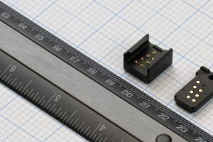
Posted on 2nd December 2024 | Modified on 2nd December 2024
Memory, Products
Memory tokens and receptacles in the Datakey Bar series now include the Mini-Bar which has been designed by ATEK Access Technologies to provide a memory system for handheld applications. The portable memory tokens and mating receptacles are more than 60% smaller than the equivalent Bar receptacle models, said the company. There are two versions available. The MBRHN has an eight-pin ...
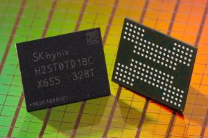
Posted on 11th August 2023 | Modified on 23rd June 2025
Business, Memory
Hynix was showing off a sample of its 321-layer 1Tb TLC NAND chips at The Flash Memory Summit earlier this week, though volume production isn’t due until 2025. Hynix used a CMOS under Array (CuA) technology which involves moving the peripheral circuitry under the cells. The company calls its peri under cell (PUC) technology ‘4D NAND’. It is not revealed ...
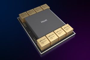
Posted on 31st July 2023 | Modified on 18th June 2025
Business, Memory
Micron has begun sampling an 8-high 24GB HBM3 Gen2 memory with bandwidth greater than 1.2TB/s and pin speed over 9.2Gb/s. It is built on Micron’s 1β (1-beta) DRAM process node, which allows a 24Gb DRAM die to be assembled into an 8-high cube within an industry-standard package dimension. A 12-high stack with 36GB capacity will begin sampling in Q1 ...
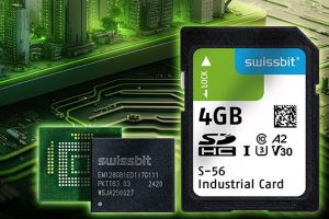
Posted on 28th June 2023 | Modified on 28th June 2023
Memory
Swissbit, the Swiss industrial storage and security specialist, is introducing e.MMCs and SD memory cards with capacities ranging from 4 to 8GB. They are based on 3D-TLC-NAND and optimised for power failure protection, industrial reliability, and high endurance, says the company, which suggests IIoT and smart city applications. e.MMC EM-30 Taking the two products in turn, the Swissbit EM-30 (153 ...
Posted on 26th April 2023 | Modified on 28th July 2023
Embedded Systems, Memory
Weebit Nano firmly believes that ReRAM technology is reaching an industry tipping point. Caroline Hayes joined the company at Embedded World to check its progress. In Nuremberg, Weebit Nano was able to demonstrate its first Resistive RAM (ReRAM) product, the S130 ReRAM module, available from US fab SkyWater. The module, based on SkyWater’s 130nm CMOS process, is a big step ...
Posted on 5th April 2023 | Modified on 5th April 2023
Business, Memory, Research
Lancaster University is creating a spinout company to develop a universal memory called ULTRARAM. Invented by Physics Professor Manus Hayne (pictured) ULTRARAM is a novel type of memory that combines the non-volatility of a data storage memory, like flash, with the speed, energy-efficiency and endurance of a working memory, like DRAM. To do this it exploits quantum resonant tunnelling in ...
Posted on 3rd April 2023 | Modified on 3rd April 2023
Memory
Scaling and wafer bonding in a cooperation between Kioxia and Western Digital have created a “218 layer 3D flash 1Tbit triple-level-cell and quad-level-cell with four planes, and features lateral shrink technology to increase bit density by over 50%,” according to Kioxia. Co-developed CBA (CMOS directly bonded to array) technology allows CMOS wafers and cell array wafers to be optimised and ...
Posted on 21st March 2023 | Modified on 21st March 2023
Internet of Things, Memory
GigaDevice is aiming at processors with a 1.2V core voltage with a family of 1.2V SPI NOR flash ICs. Called the GD25UF series, they run from 1.14V-1.26V and “provide for a simpler power system architecture, and for direct interfacing between the I/O pins of the SoC or processor and the GD25UF device”, according to the company. The 64Mbit GD25UF64E is ...