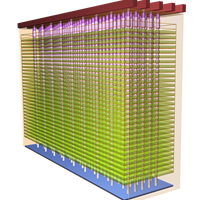
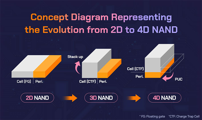
Hynix used a CMOS under Array (CuA) technology which involves moving the peripheral circuitry under the cells. The company calls its peri under cell (PUC) technology ‘4D NAND’.
It is not revealed whether Hynix used string stacking – which puts one or more 3D NAND devices on top of each other and connects them to make the 321-layer memory – but since this is how it made its 238-layer memory which went into production in June, it is possible.

At this year’s ISSCC, 35 Hynix engineers presented a paper in which they described how they applied five new techniques to a 300-layer 1Tb TLC 3D-NAND flash memory product:
- A triple verify program (TPGM) technique is used to improve program performance.
- An adaptive unselected string pre-charge (AUSP) technique is used to reduce disturb and program time (tPROG).
- A programmed dummy string (PDS) technique is used to reduce WL settling time.
- An all-pass rising (APR) technique is used to reduce the read time (tR),
- A plane-level read retry (PLRR) technique is used during erase to improve the QoS.
The TPGM scheme reduces tPROG by narrowing the cell threshold voltage (VTH) distribution. SK hynix’s current double-verify program (DPGM) scheme divides cells into three groups while TPGM categorizes cells into four groups and so is better able to manage their program (write) performance. This “results in approximately a 10 percent of program time reduction,” the paper states.
The AUSP technique shortens program time by another 2 percent, we’re told. The PDS scheme contributes by reducing the capacitive load affecting the wordline’s settling time. The APR scheme reduces the wordline’s response time to a new voltage level, and improves read time by 2 percent.
The cumulative effect of these gains is a 1Tb 300+ layer TLC NAND cell with a 20Gb/mm2 bit density and a 194GBps write speed