Infineon to sample first GaN ICs made on 300mm wafers in Q4

Infineon will sample customers with GaN chips made on 300mm wafers in Q4.

“Our fully scaled-up 300mm GaN manufacturing will allow us to deliver highest value to our customers even faster while moving towards cost parity for comparable silicon and GaN products,” says Infineon’s Johannes Schoiswohl. Infineon uses Si, SiC and GaN for power ICs.

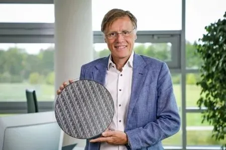
Infineon’s CEO Jochen Hanebeck (above) holds a 300mm GaN wafer

Infineon claims to be first to develop 300mm GaN power wafer technology. Chip production on 300mm wafers is technically more advanced and s efficient compared to  200mm wafers.

The company has launched over 40 GaN products  in the past year.

David Manners

David Manners

David Manners has more than forty-years experience writing about the electronics industry, its major trends and leading players. As well as writing business, components and research news, he is the author of the site's most popular blog, Mannerisms. This features series of posts such as Fables, Markets, Shenanigans, and Memory Lanes, across a wide range of topics.

Leave a Reply

Your email address will not be published. Required fields are marked *

*