“The G1719x series are near-infrared sensors offering high sensitivity and low dark current, comparable to conventional metal packages, while featuring a surface-mounted ceramic design compatible with lead-free re-flow soldering,” according to the company. They are “tailored to meet the needs of researchers and engineers across industries including gas sensing, remote temperature measurements and laser applications”.
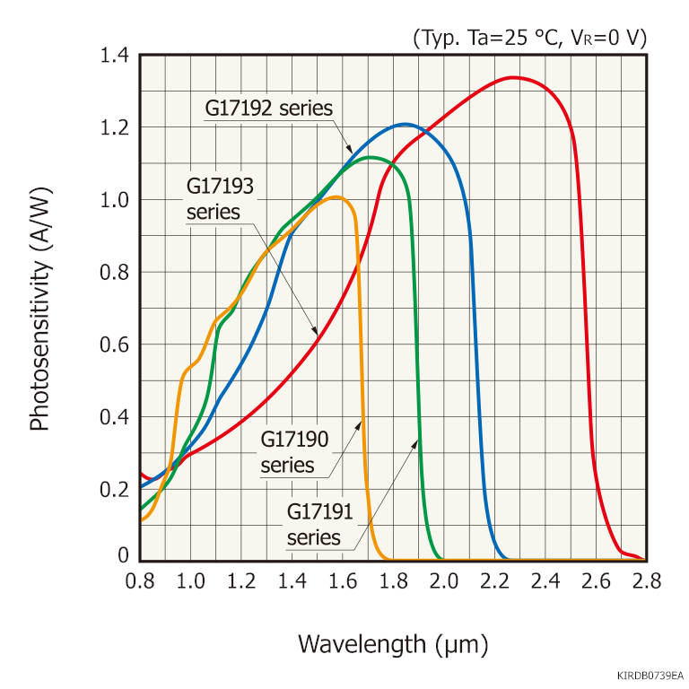
T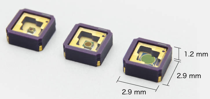 here are three wavelength ranges: 0.9 to 1.7μm (1.55μm peak), 0.9 to 1.9μm (1.75μm peak), 0.9 to 2.1μm (1.95μm peak) or 0.9 to 2.6μm (2.3μm peak), and three photo diode diameters*: 0.3. 0.5 or 1.0mm. All combinations are available.
Packaging is 2.9 x 2.9 x 1.2mm, with light entering perpendicular to the PCB.
Low dark current and high sensitivity are claimed, but the company is not making these figures public yet.
*the company describes these as ‘area’ not diameter. Electronics Weekly is checking which is true.
| Type G1719…. |
Photosensitive diameter* (mm) |
Spectral response (μm) |
Peak sensitivity wavelength (μm) |
|---|---|---|---|
| …0-003K | 0.3 | 0.9 to 1.7 | 1.55 |
| …0-005K | 0.5 | ||
| …0-010K | 1.0 | ||
| …1-003K | 0.3 | 0.9 to 1.9 | 1.75 |
| …1-005K | 0.5 | ||
| …1-010K | 1.0 | ||
| …2-003K | 0.3 | 0.9 to 2.1 | 1.95 |
| …2-005K | 0.5 | ||
| …2-010K | 1.0 | ||
| …3-003K | 0.3 | 0.9 to 2.6 | 2.3 |
| …3-005K | 0.5 | ||
| …3-010K | 1.0 |