Typical gate-drain charge is 37nC (400Vd, 10Vg, 80A) and total gate charge (gate-source + gate-drain) is 140nC.
Reverse recovery for the intrinsic diode is 8.5µC and 425ns, both at 400V, 40A, 100A/µs and Vg=0 .
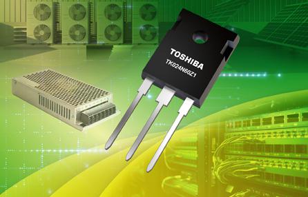
“TK024N60Z1 uses the DTMOSVI 600V process to achieve low on-resistance and reduced conduction losses,” according to the company. “This reduces drain-source on-resistance per unit area by approximately 13%. More importantly, drain-source on-resistance times gate-drain charge is reduced by approximately 52% compared to Toshiba’s DTMOSIV-H products with the same drain-source voltage rating.”
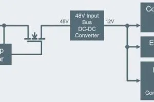
Applications are foreseen in data centre servers, industrial equipment and photovoltaics.
The company has a G0 Spice model for circuit function verification, and a more accurate G2 Spice model that includes transient characteristics.