Not only that, but it needs no trimming, reference voltage nor supply regulation, and it works over -25 to 75°C.
Operation indoors from a 1mm2 solar cell has been demonstrated “under any practical lighting condition”, according to the presentation at ISSCC.
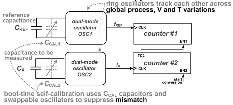 The capacitance to digital converter is built around a pair of nominally identical relaxation oscillators, each feeding its own counter.
One oscillator uses the capacitance-under-test as its frequency-determining component, and the other uses a reference capacitor.
At the end of a conversion cycle, the ratio of the two counts is proportional to the ratio of the known and unknown capacitors.
As resolution is better if the higher count is on the denominator of that division, provision is made for to swap the capacitor connections so that the smallest (highest frequency) one is always linked to the counter that acts as the denominator. Swapping happens if an initial conversion cycle shows the larger capacitor is on the wrong channel.
In effect, each channel consists of: a capacitor, a cross-over switch, an oscillator and a counter.
Calibration is performed by operating a further change-over switch that temporarily swaps the counters between the oscillators – so a more accurate way to describe the arrangement is:
capacitor-switch-oscillator-switch-counter.
It transpires that, by examining counts after both front-end capacitors are swapped and counters are swapped, it is possible to detect all the offsets in the signal chains and use that information to compensate for them – by electrically connecting some small fixed capacitors (down to 10fF) across the oscillator input nodes.
“The CDC is inherently insensitive to global process, voltage and temperature variations, as they equally affect the capacitance-to-period conversion gain” in each channel, according to the ISSCC presentation.
Built by TSMC with a 180nm chip process, the circuit occupies 0.2mm2 and the capacitance-under-test can range across 0 to 30pF. Nominal resolution is 125fF. Noise limit is 45.7fFrms (0.36 of a bit). Maxmum INL after self-calibration is 125fF – one bit.
ISSCC 2021 Paper 5.2: Capacitance-to-digital converter for operation under uncertain harvested voltage down to 0.3V with no trimming, reference and voltage regulation
The illustration is copied from the ISSCC Digest, paper 5.2, with permission