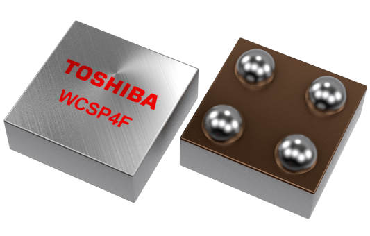
Called the TCR5RG series, the low drop-out parts cover an output voltage range of 900mV to 5V.
Achieved through the combination of a wide-gap internal circuit topology, an integrated high-speed operational amplifier and low-pass filtering, according to the company, typical ripple rejection (2.8V type, according data sheet) is:
- 100dB at 1kHz
- 93dB at 10kHz
- 67dB at 100kHz
- 59dB at 1MHz
Internal low-pass filtering turns on ~2ms after output is established.
There are 45 different devices, which typically have 5μV output noise, and support outputs up to 500mA – typical drop-out for 2.8V part at 500mA is 150mV.
Operation is over -40 to +85°C, and 1.8 to 5.5V (with drop-out and temperature caveats on voltages).
Power dissipation can be as high as 800mW – on 40 x 40mm FR4 with plenty of copper on both sides and a lot of vias.
Quiescent current is typically 7μA with no load, and there is a shut-down pin to take this to ≤below 1μA and typically 80nA at 25°C.
Output accuracy is ±1.5% output voltage (1.8 to 2.8V) or ±1.8% (>2.8V). Below 1.8V the spec is ±36mV.
Input and output capacitors have to be added – 1μF for each, ceramic capacitors can be used.
Devices are available with and without active discharge on the output.
Key uses, said Toshiba, include phones, sensor-based system, IoT-chipset, RF systems, wearable technology, portable audio equipment, and healthcare monitoring units.