Home » News » Research (page 32)

Research

The latest electronics research news from within the industry and universities from around the world.

Surrey University hooks up with Viavi on 6G

9C180F1F-D484-4700-B571-2104CE6CFC93-300x200.jpeg

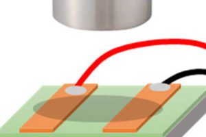
Viavi Solutions is supporting 6G academic and industry research worldwide through its new 6G Forward program. The program is designed to provide vital expertise, technology, and funding to promising avenues of research, which may lead to breakthroughs for the next generation of wireless technology. At the University of Surrey, Viavi is a founding member of the 5G/6G Innovation Centre led ...

Piezoelectric transistors for force sensing?

NCKU piezo gated thin film transistor force sensor

National Cheng Kung University in Taiwan is experimenting with piezoelectric gated thin-film transistors. “Piezotronic force sensors are typically governed by either a strain-induced Schottky barrier height modulation or by a piezo-gating effect that redistributes the charge carriers in an induced piezoelectric field,” according to NCKU. “While Schottky barrier height based piezotronic devices have been well-explored, piezo-gating based devices remain relatively ...

Drones auto-navigate through complex environments at high speed

UZH drone flight

The University of Zurich is teaching drones to fly at the highest possible speed thorough complex environments. “Our algorithm leverages classical topological path planning and deep reinforcement learning,” according to the University’s Robotics and Perception Group. In the first step, (right) many collision free paths are found using a probablistic rodmap method. After this, the paths are filtered with different ...

Five year life for perovskite solar cell, and a way to accelerate life testing

Princeton-30yr-Perovskite-Solar-Cell

Princeton University is predicting five years, and maybe 30 years, of outdoor life from a Perovskite solar cell stack-up invented in its labs. The key is a 2D material barrier layer between the photon-absorbing perovskite layer and the hole transport layer. “While the idea of a 2D capping layer isn’t new, it is still considered an emerging technique,” according to ...

Gradient doping improves triboelectric nano-generators

GISTT-triboelectric-improvement-931-300x200.jpg

Graduated charge-confinement could be the key to much improved triboelectric nano-generators (TENGs), according to the Gwangju Institute of Science and Technology and Chonnam National University in Korea, which have been working on suitable structures. Triboelectric generators produce power through electrostatic induction when dissimilar insulating materials are brought together and parted (right, and far below). Two of the things that push ...

UV-NIL extended to below 10nm

FE20ACF7-23AE-4499-9A43-5633EC7A6807-300x200.png

Researchers from Tokyo University have uncovered molecular properties that help fill nanometer-sized gaps in the nanopatterning mould for ultraviolet nanoimprint lithography. Ultraviolet nanoimprint lithography (UV-NIL) is a method of creating patterns at the nanoscale with widespread applications in optoelectronics, photonics, and biology due to its low cost and scalability. However, current UV-NIL resolution is limited below 10 nm, and higher ...

Protonic gate spintronics – a tool for low-power ‘electronics’ beyond CMOS?

RMIT vanDerWaals vdW heterostructure device

Electric gate-controlled exchange-bias effect in van der Waals heterostructures has been has observed for the first time, according to RMIT University in Australia, which describes the effect as “a promising platform for future energy-efficient, beyond-CMOS electronics”. “To date, very limited electrically tunable exchange-bias effects have been experimentally demonstrated in some oxide multi-ferroic thin film systems”, according to the university, but ...

More optically-active 2D heterostructures from Monash University

Monash 2d perovskite_paper-2 lo

Monash University as been looking into stacks of differing 2D materials with the Indian Institute of Technology Bombay, yesterday revealing tuneable photon absoption from perovskites layered with transition metal dichalcogenides. At the same time, the team revealed two other optically-active 2D parings: WSe2 – SnSe2, and black phosphorous with MoS2. All the pairings are held in stacks by van der ...

Dissimilar 2D materials stack harmoniously to turn photons into electrons

Monash 2d perovskite TDM heterostructure

The interfaces in assemblies of 2D materials could produce opto-electronics devices, according to Monash University in Australia, which is designing them using density functional theory (DFT) based band-structure modelling. “2D perovskites show interesting photo-physical properties and better stability compared to typical bulk perovskites,” according to Monash. “However, till now, near-infrared and visible-range optoelectronic device performance metrics of 2D perovskites have ...

Crab-inspired image sensor works on land and in water over 360°

GIST artificial crab eye camera

The eye of the fiddler crab has inspired an artificial image sensor that works on land and in water without refocusing. This crab moves freely between aquatic and terrestrial environments, and to be effective in both its eyes have flat corneas with a graded refractive index profile, according to the Gwangju Institute of Science and Technology in Korea, where the ...