Home » Tag Archives: transistor

transistor

Imec transistor for 6G FR3 band

IMG_0784-300x200.webp

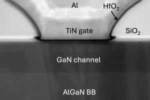
Imec has developed a GaN MOSHEMT on silicon that achieves both record efficiency and output power for an enhancement-mode (E-mode) device operating at low supply voltage. In parallel, imec also demonstrated a record-low contact resistance of 0.024Ω· mm which is essential to further boost output power in future designs. The results mark a crucial step toward integrating GaN technology into ...

Someone, please explain how this two-npn voltage reference works

EinW odd Vref LM311 data sheet

I was digging around in the LM311 (and LM111, LM211) comparator data sheet, and came across this unusual voltage reference (diag right). It consists of an npn cascsode pair of transistors, the top one connected (collector to base) as a diode, and the two bases tied together. I have no idea how this works, and am going slightly bonkers trying ...

PCIM: Navitas optimises SiC for speed

Navitas gen3F SiC mosfets

Navitas Semiconductor has made fast versions of its Gen-3 650 and 1,200V silicon carbide mosfets, branded ‘G3F’ and available in packages including D2PAK-7 to TO-247-4. “We’re pushing the boundaries of SiC, with up to 600kHz switching speeds said company v-p of technology Sid Sundaresan. One proposed application is in continuous-conduction-mode totem-pole power factor correction (CCM TPPFC) circuits up to 10kW in ...

Solid-state ‘thermal transistor’ controls heat flow with ±2.5V

Carborane cage atom has tuned thermal conductivity

UCLA researchers have made an electrically-controlled solid-state ‘transistor’ for thermal energy, with a heat-flow on-off ratio of >13:1 when controlled with a ±2.5V base bias at room temperature. The voltage-flow curve is almost a straight line, and operation at 1MHz has been demonstrated. “Precision control of how heat flows through materials has been a long-held but elusive dream for physicists ...

Fast solid-state neuromorphic proton transistor trained to convert triangles into sinewaves

NIMS UTokyo neuromorphic transistor

Japan’s National Institute for Materials Science (NIMS) and the Tokyo University of Science have created a solid-state electric double layer neuromorphic transistor, claiming it to be the fastest yet, and proving its computational ability by training it to convert waveforms. “The team measured the speed at which the transistor operates by applying pulsed voltage to it, and found that it ...

Get high mobility and high stability in display-grade TFTs

ChineseAcSci CTL CRL bilayer TFT diag NIMTEimage

75.5cm2/V/s mobility and high stability are claimed for amorphous oxide semiconductor thin-film transistors created at the Ningbo Institute of Materials Technology and Engineering (NIMTE). The bottom-gate transistor is built with a stack of two layers: Next to the oxide-insulated silicon gate is a charge transport layer (CTL) consists of indium-rich InSnZnO “featuring large average effective coordination numbers for all cations ...

ISSCC 2023: 2D materials instead of silicon in the angstrom era?

ISSCC27.3 Imec dichalcogenide transistor physical

At ISSCC 2023 in San Francisco, Belgian research lab Imec presented transistor designs shrunk beyond the capabilities of silicon. It argued that finfet and gate-all-around designs can only go so far with silicon as, to get fast access to the carriers inside a channel, the channels have to be so thin that physics takes its toll. At <3mn, thickness variations ...

Piezoelectric transistors for force sensing?

NCKU piezo gated thin film transistor force sensor

National Cheng Kung University in Taiwan is experimenting with piezoelectric gated thin-film transistors. “Piezotronic force sensors are typically governed by either a strain-induced Schottky barrier height modulation or by a piezo-gating effect that redistributes the charge carriers in an induced piezoelectric field,” according to NCKU. “While Schottky barrier height based piezotronic devices have been well-explored, piezo-gating based devices remain relatively ...

40V bi-direction GaN transistor for power rail switching

Innoscience bidirectional GaN

Chinese GaN device maker Innoscience is introducing a bi-directional transistor amongest its more conventional devices. Called INN40W08, it is a 40V device that can block in both directions (unlike single silicon mosfets where two are needed for bi-directional operation). Innoswitch announced an up-dated version here Nominally it has a gate, two drains and no source. The company sees it being ...

6mΩ 750V SiC FET from UnitedSiC 

UnitedSiC-6mohm-750V-SiC-cascode-application-300x200.jpg

A 6mΩ 750V SiC transistor is amongst nine devices announced by UnitedSiC. The company decribes the transistors as ‘FETs’, although each is a co-packaged cascode pair of a depletion-mode high-voltage SiC JFET and a low-voltage silicon mosfet. “At a Rds(on) of less than half the nearest SiC mosfet competitor, the 6mΩ device also provides a short-circuit withstand time of 5μs,” according ...