Home » Tag Archives: stacked die

stacked die

3d stacked integration for DRAM and processors

InstOfScienceTokyo BBCube 3d stacked integration

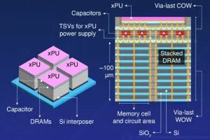
Institute of Science Tokyo revealed advances to its BBCube 3D integration process at ECTC, the IEEE Electronic Components and Technology Conference. “These new technologies can help in addressing the demands of high-performance computing applications which require high memory bandwidth and low power consumption with reduced power supply noise,” according to the Institute. BBCube stacks a processor on top of a ...

Leti 3D chip technology gets big push from Qualcomm

Leti-s-White-Room-300x200.jpg

A 3D chip technology, which stacks active layers of transistors without the need for through-silicon vias (TSVs) has been developed by Leti and is the focus of a collaboration with Qualcomm. Dubbed CoolCube, the  French research centre has developed a device scale-stacking technology for complex system-on-chips such as mobile processors which is why Qualcomm is collaborating with Leti. The technology ...

High speed stacked memory arrives with HBM standard

proGraphic3-300x100-300x100.jpg

A stacked memory device which has the potential to achieve memory access speeds 14 times faster than today’s DDR4 has been demonstrated by eSilicon, Northwest Logic and SK Hynix. The stacked memory device is complaint with the JEDEC 2.5D packaging standard known as high bandwidth memory (HBM). The chip uses an FPGA-based controller core and PHY for the HBM standard architecture implemented in a Hynix ...

Toshiba stacks 16 NAND die using TSVs

Toshiba-x16-stacked-nand-flash-300x182-300x182.jpg

Toshiba has used through silicon vias (TSVs) to connect up to 16 stacked die in a range NAND flash chips. The prototype will be shown at Flash Memory Summit in Santa Clara next week. “Prior art stacked NAND flash memories are connected together with wire bonding in a package,” said the firm. “TSV technology instead utilises the vertical electrodes and ...