L-R: Kari Hjelt, Chalmers University, Gordon Rinke, AMO, Salim El Kazzi, Aixtron, Dr Amaia Zurutza, Graphenea,
One of the partners, Graphenea, manufactures and commercialises different graphene materials. Its scientific director, Dr Amaia Zurutuza confirmed that the project has evolved from 100mm graphene on copper wafers, which was suitable for initial customers which were researchers at universities. Now, 150 and 200mm wafers are being produced for prototyping.
In 2018, Graphenea decided to fabricate graphene transistors on a commercial scale to commercialise a more elaborate product “to make [customers’] life easier so they could focus on their applications,” said Zurutuza.
Part of the progress made since 2020 was to use exisiting tools and develop new processors to realise the commercial production of 200mm and 300mm wafers for electronics, photonics and sensor applications.
Partner Aixtron has developed a new tool for transferring the thin, one atom, transparent graphene layer to the substrate. this is already in use at partner imec’s facility and producing “a lot of wafers”.
Salim El Kazzi, Aixtron’s2D product manager, added that the project is aiming for fab-compatible 2D integration with samples of 300mm sapphire wafers and the first 2D growth on 700mm sapphire wafers.
He added that future challenges are handling and cleaning and defining a methodology to advance these 2D materials into the silicon industry.
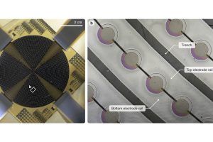
The first phase of the 2D-EPL project is to offer integration services with multi-purpose wafer (MPW) runs with process design kits. Customers can take a portion of a single wafer as part of the prototyping process to optimise the costs of prototyping.
Zurutuza confirmed that the price for a 4cm2 wafer (i.e., 4x 1cm x 1cm2 dies or 16x 5cm x 5mm2 dies) is €3900.00. The backgate metal is Ti/Au with an HfOx 20nm backgate dielectric and a CVD grown graphene monolayer. There currently six MPW runs which can implement three types of devices within one process flow.
The project will introduce a design freeze from 15 July, with tapeout and the delivery run set for 01 September 2024.