The transistor is integrated within Power Integrations’ latest series of InnoMux 2 branded multi-output flyback ac-dc converter ICs, in this case it is intended to work from 1,000V rails in industrial applications.
“InnoMux 2 is the first vehicle because a lot of applications that need 1,700V are industrial with two or three outputs” says director of training Andy Smith.
The transistor has been developed within the company and is a cascode device, made on a bought-in wafer, whose epitaxy is grown in-house.
That is all the company would reveal: whether it is GaN-on-silicon or not, and where the fab is, remain undisclosed.
The motivation for high-voltage GaN here is simply cost saving, says Smith: silicon carbide [SiC] transistors, which the company already uses in high-voltage products (and will continue to used in those products, he said), are expensive because the boule from which wafers are sliced takes so long to grow.
Are the 1,700V GaN transistors fast?
“There is no need for speed in flyback. We don’t run more than 140kHz anyway” responds Smith. “We can run at 300kHz, but the need for creepage and clearance means magnetic core volume does not scale 2:1.”
GaN transistors lack the avalanche-based over-voltage protection that can be designed into silicon or silicon carbide mosfets.
Instead, GaN transistors are designed with a large over-voltage margin – margin that has yet to be standardised between manufacturers.
How does it handle Rds?
“Our GaN devices break down around twice the rated voltage,” says Smith. Above the rated voltage “a high-voltage spike causes electrons to shoot out of the channel into surrounding GaN, imparting a charge and inhibiting the channel – Rds(on) increases by 4-5%. The electrons will drift back eventually, and Rds(on) gets back to normal over a number of hours. This is non-destructive until 2x the rated voltage.”
Is the result as tough as a SiC dc-dc converter?
“Silicon carbide is exceptional,” says Smith. “I think GaN is more resilient than silicon.”
How is reliability?
“We have 14 product families that use GaN, and we have developed a good set of reliability data, accelerated by high-temperature and high voltage,” says Smith. “Our FIT is around 0.9.”
(FIT is ‘failures-in-time’, and is calculated here assuming 55°C and 0.7eV activation energy at a 60% confidence level.)
Are standard heat and voltage acceleration techniques valid for GaN?
“The Arrhenius equations holds true for GaN as well as silicon if you don’t go too far,” says Smith.
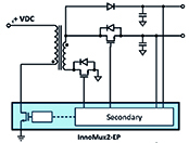
Figure 1
InnoMux is the company’s multi-output flyback dc-dc architecture and it has sized its first 1.7kV GaN transitor product for outputs up to 100W, making it suitable for industrial auxiliary power supplies, (see Figure 1).
The topology works using a single primary-side switch – the GaN HEMT in this case – and one or two secondary-side low-voltage mosfet switches – one for a dual output and two for a triple output.
The highest voltage output has no controlling series switch, allowing the one or two secondary mosfets to ‘steal’ power for their outputs when needed. This can happen for all outputs during each primary switching cycle.
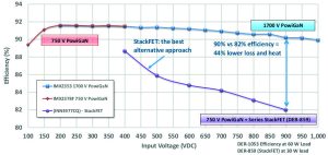
Figure 2
The control IC contains both primary and secondary control die, an inductive isolated feedback link, and the GaN primary switch. All output voltages can be regulated to within 1%.
This primary switch is exposed to the input voltage, plus the output voltage reflected back through the turns ratio, plus any switching and rectifier recovery transients, (see Figure 3).
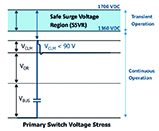
Figure 3
These add up to less than 1,360V in the company’s 1,000V input RDR-1053 design example and report, says Smith, leaving 340V of clear headroom for unexpected transients before the transistor experiences even temporary Rds(on) changes.
RDR-1053 describes a 60W dc-dc with two outputs: 5V and 24V.
Efficiency tests have been done comparing the company’s earlier 750V GaN transistor and its ‘StackFet’ switch, which stacks a high-voltage silicon mosfet on top of the 750V GaN transistor in series.
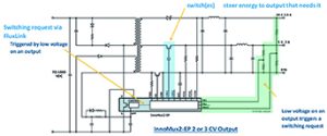
Figure 4
Using the same PCB and inductors (see Figure 2), efficiency remains above 90% for inputs between 150V and 1kV with the 1,700V GaN transistor, and is identical to efficiency for the 750V transistor with inputs up to 400V.
Just like the 1,700V GaN version, the StackFET dc-dc converter also works with inputs up to 1kV, but sacrifices 2% in efficiency at 400V, increasing steadily to 8% at 1kV.
Silicon carbide tests have yet to be done as the necessary one-off SiC InnoMux 2 circuit has to be constructed, says Smith, but “I expect SiC would be similar to the 1,700V GaN results.”