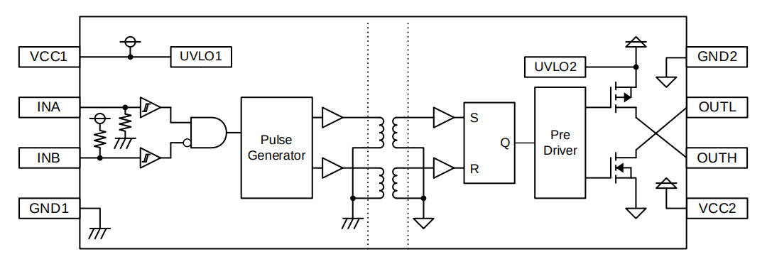
Made by Rohm and called BM6GD11BFJ-LB, they have “an isolation voltage of up to 2,500Vrms, a minimum input-output latency of 60ns and a minimum input pulse width of 65ns”, said Rutronik. “Under-voltage lock-out is integrated into the input side and the output side, [and] the drivers operate over -40 to +125°C.”
On the input side, 5V power is needed with consumption between 250μA and 6mA depending on the device and what it is doing.
There are two logic inputs to give a choice of inverted or non-inverted pulse streams, with the unused pin available as an inhibit.
Input logic thresholds are 2.0V min for high and 0.8Vmax for low, and input resistors are provided to set the output side GaN transistor off should the inputs be disconnected.
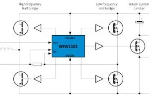
A separate floating power supply is needed for the output side of the IC at between 4.5 and 6V relative to the GaN transistor source. Power needs will depend on driven conditions.
This secondary voltage needs to suite the gate requirements of the particular GaN transistor – which are always fussy – and can be supplied by bootstrapping for half-bridge high-sides, although regulation will probably be needed.
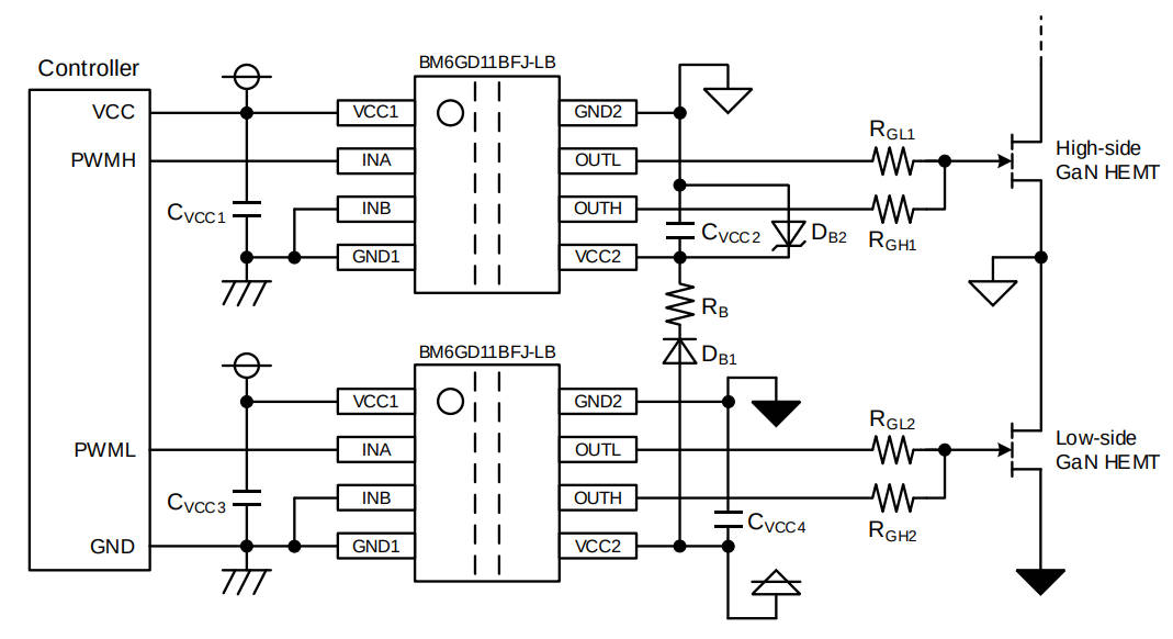
There are two separate outputs to allow separate resistors to independently set the turn-on and turn-off times of the driven hemt. Typically, the internal 1.35Ω source resistance and 800mΩ sink resistance make 3A of pull-up and pull-down output current available (2A minimum).
Input-side under-voltage lock-out is typically centred on 3.45V, and the output-side is typically centred on 4.05V
Inside, signal isolation is inductive, with separate transformers passing across the rising and falling edges. A flip-flop reconstructs the pulse stream on the secondary side.