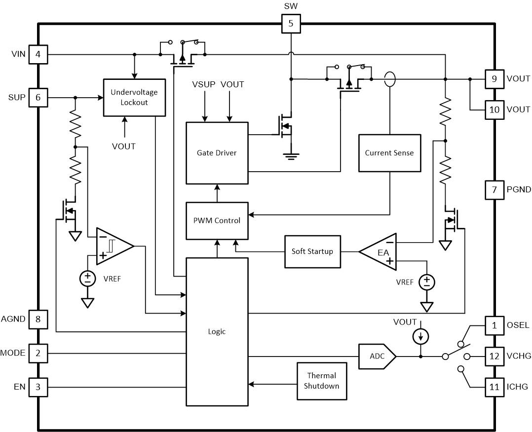
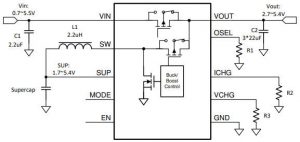
All the time sufficient voltage is available at the input, the input is connected directly (with no regulation) to the output to feed the load and a buck converter keeps the capacitor charged.
Data sheet typical application 2 – scroll down for a note on this diagram
When the input drops below a threshold, it is disconnected and the load is instead powered from the supercapcitor via the dc-dc converter, now in boost mode.
Update: “The switchover will be very fast and seamless. From an application perspective it will be like an instantaneous mode change,” TI told Electronics Weekly. End update.
 Data sheet typical application 1
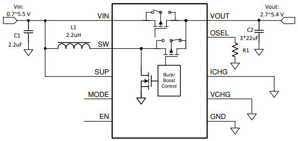
The chip can also be without a supercapacitor, but with the boost converter connected to the input (circuit right).
“Output current depends on the inductor current limit and the input voltage,” TI told Electronics Weekly. Without the supercapacitor it “can support 250mA Iout from 0.7Vin from a source connected to the TPS61094” (right) or it “can support the same output current from a supercapacitor” (above left).
Sixteen internal settings are available each for charging termination voltage (1.7-5.2V), charging current (2.5-600mA or off) and output voltage during back-up (2.7-5.4V), set via a 4bit ADC by the values of resistors connected to pins Vchg, Ichg and Osel respectively. These resitors are only read at power-up or after the enable pin is toggled.
Once the back-up capacitor is charged, the chip will keep working regardless of input voltage, so long as there is at least 700mV across the capacitor. For start-up, there is a ~1.7V under-voltage lock-out on the input pin.
Called TPS61094, it has three other modes, set by the states of the ‘enable’ pin and ‘mode’ pin.
- Auto – described above. The back up capacitor is used when the input drops to within 100mV of the back-up output voltage.
- Forced buck – the supercapacitor is charged, but not used for back-up
- Forced bypass – the bypass mosfet is on full-time and the converter is off to save power. No protection against reverse current from output to input
- True shutdown – the input, load and capacitor are disconnected from each other
Shutdown is automatically entered if the input and capacitor are below ~1.7V and the output is below ~1.6V.
Quiescent current with all these inputs and outputs varies with mode and can be as low as 60nA typical (and as high as 550nA max) depending on the pin and the mode.
Packaging is 2 x 3mm, 12pin thin WSON.
TPS61094EVM-066 evaluation module is available.
Use is foreseen in smart utility meters, and other low-power applications where output current peaks are expected from radio loads such as narrowband IoT, LTE-M, Wi-SUN, MIOTY, Bluetooth and wireless M-Bus, said TI.
The TPS61094 product page is here and the data sheet is here
Note on the typical application diagram above:
TI has labelled the Vin range as ‘0.7-5.5V’. Electronics Weekly has asked TI why this is not 0 to 5.5V.
Also, for current to be drawn from the input source, as far as Electronics Weekly can tell (do check the data sheet), the input voltage has to be higher than the output set voltage if the capacitor is charged, or higher than the instantaneous capacitor voltage, or higher than the Vin under-voltage lock-out voltage if the capacitor is discharged.