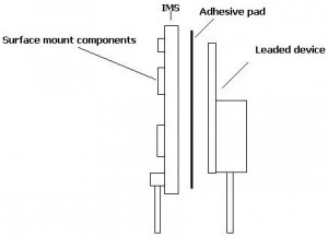
In particular, it applies to a daughter-board with mixed surface-mount (SMD) and through-hole components, that is soldered vertically into into a horizontal power supply motherboard.
The reason for mixing through-hole and SMD components is that leaded power transistor packages, like TO-220s, despite their age, have advantages when plenty of current must be handled.
“Although power semiconductors are available in surface mount packages, it is easier to transfer high currents to the main [mother]board with a leaded part,” said TDK. “This alleviates the need for multiple low current pins on the lead-frame, occupying valuable board area. Surface mount I2PAK packages with leads to carry the high currents to the main board are available, but are expensive.”
However, TO-220 packages require fastening to the heatsink, so SMD power components are easier to use when less current is needed.
“Consequently, a combination of both surface mount and leaded components are generally required,” said TDK.
Developed by TDK-Lambda engineer Martin Coates, the firm’s answer is to surface-mount the medium power components on the PCB side of an insulated metal substrate (IMS) (see diagram), then mount TO-220s and similar through-hole packages on the plain back side using thermal adhesive tape.
Diagram note: it is not to scale and the thermal tape is shown far thicker than the Bergquist Bond-Ply 100 suggested in the patent.
Adhesive removes the need for screw fastening which would waste space on the SMD side.
By mounting the TO-220s close to the bottom edge of the daughter board, and using a surface-mount 90deg header on the bottom of the other side, the daughter board becomes a dual-in-line sub-assembly for the motherboard.
The patent also covers direct copper bonded (DBC) and alumina substrates, and alternatives to adhesive tape mounting.
 Electronics Weekly
