Wafer
Wafers are the foundation of semiconductor manufacturing, where process nodes, materials, and fabrication technologies define chip performance. Innovations in 3D stacking, SOI wafers, and GaN/SiC substrates are expanding design possibilities for power electronics, RF, and high-speed logic. Wafer-level packaging (WLP) and foundry advancements are also transforming system integration. Wafer news delivers critical updates for professionals tracking the evolution of fabrication processes, supply chain capacity, and materials science in the global chip industry.
Posted on 4th June 2025 | Modified on 4th June 2025
Business, Manufacturing
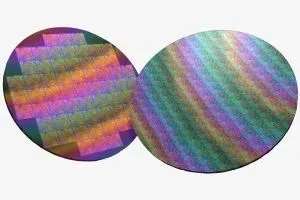
Soitec, the French wafer manufacturer, has announced a strategic collaboration with Powerchip Semiconductor Manufacturing Corporation (PSMC). Soitec will supply PSMC 300mm substrates incorporating a release layer, Transistor Layer Transfer (TLT) ready, to support a new demonstration of advanced 3D chip stacking at the wafer level. This marks the first public announcement of Soitec’s TLT technology. The technology is an enabler ...
Posted on 2nd April 2025 | Modified on 2nd April 2025
Discretes, Finance, Manufacturing, Power, Power Supplies
Power mosfet and wafer-maker IceMos Technology has pulled-in $22m of series-E funding, including $7.5m from 57 Stars, and money from un-named “earlier stage USA investors” and a “London-based investor”, said IceMos Headquartered in Arizona, IceMos has manufacturing in Northern Ireland, research in Arizona and a design center in Tokyo. Its wafer products include active layers attached to handle wafers using ...
Posted on 1st August 2023 | Modified on 24th June 2025
Research
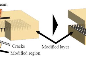
Chiba University has found a way to cut blocks of diamond into thin wafers along a difficult but desirable crystal plane using lasers. The ‘100’ plain leaves a surface that is relatively easy to planarise and etch for semiconductor use, according to the Chiba researchers, but diamond wants to crack along its 111 plane, so any crack-based separation starting in ...
Posted on 27th July 2021 | Modified on 28th July 2021
Manufacturing
STMicroelectronics has manufactured its first 200mm silicon-carbide bulk wafers at its Norrköping Sweden facility. “The transition to 200mm SiC wafers will bring substantial advantages to our automotive and industrial customers as they accelerate the transition towards electrification,” said ST president of automotive Marco Monti. The company is claiming high quality with minimal crystal-dislocation defects through expertise in SiC ingot growth technology ...
Posted on 19th November 2019 | Modified on 19th November 2019
Automotive Electronics, Manufacturing
ST Microelectronics has extended its multi-year silicon carbide wafer deal with Cree, taking it to over $500m in total value. Cree will supply 150mm bare and epitaxial silicon carbide wafers to ST over “several years”, according to Cree. “Expanding our long-term wafer supply agreement with Cree will increase the flexibility of our global silicon carbide substrate supply,” said ST CEO Jean-Marc ...
Posted on 21st April 2017 | Modified on 11th May 2017
Research
MIT proves that semiconductor epitaxy can be performed on a graphene-coated wafer, allowing the circuit or devices to be peeled off
Posted on 30th September 2013 | Modified on 30th September 2013
Consumer
Apart from PC which is falling fast and expected to be weak for a couple more years, the trend for cosumer electronics looks good.
Posted on 25th July 2013 | Modified on 25th July 2013
Finance
ARM is enthusiastic about the potential of FD-SOI – STMicroelectronics’ process which is getting massive backing from the French government.
Posted on 25th July 2013 | Modified on 3rd June 2019
Manufacturing
ARM is enthusiastic about the potential of FD-SOI – STMicroelectronics’ process which is getting massive backing from the French government.
Posted on 9th July 2013 | Modified on 16th June 2025
Manufacturing
Next year’s fab equipment sales will be the second highest ever, says SEMI, at $43.98 billion compared to the record of $47.7 billion in 2000.