X-Fab has improved 25V isolation for better SPAD integration in its 180nm XH018 fab process. 4×3 SPAD arrays: Original Isomos1 and new Isomos2 (right) SPADs – single-photon avalanche diodes – are used as optical receivers in lidar, 3D imaging, depth sensing and quantum communication. The improved isolation module, called Isomos2, improves pixel density and fill factor. “In a typical 4×3 ...
Home » Tag Archives: Process
Process
Keep up with the latest developments in semiconductor process technology, where advancements in chip fabrication and manufacturing techniques are crucial for scaling performance and reducing costs. From 2nm , 5nm and 7nm nodes and beyond, process technology is essential for improving the speed, efficiency, and integration of semiconductors. Innovations in material science, lithography, and packaging technologies continue to reshape the way chips are designed and produced, enabling new possibilities for smart devices, AI, 5G, and quantum computing. As the semiconductor industry pushes forward – through compnaies such as ASML, Imec, TSMC, Samsung and Intel – process improvements play a key role in driving technological evolution.
Novel logic aims to beat CMOS, on 10 year older fabs
Nottingham-based SFN (Search for the Next) has characterised its novel transistor-based logic, and claims that it matches CMOS performance even when made in older fabs. It would “enable chip designers to produce ICs in older 180nm, and even one micron, geometry fabs with the equivalent performance of CMOS devices made in state-of-the-art plants”, according to the company. “For example, a ...
X-Fab adds 375V nmos and pmos super-junction transistors to BCD chip process

X-Fab Silicon Foundries has added 375V power transistors to the devices available from its 180nm deep trench isolation BCD-on-SoI platform chip fab. The second generation of its XT018 super-junction high-voltage primitive devices, they cover 45 to 375V in one process module and are aimed at applications like medical ultrasound transmitter-receiver ICs and AC line-powered IoT sensors. The complementary nmos-pmos devices qualified ...
X-Fab adds photodiodes to 180nm process, from UV to near-IR
X-Fab Silicon Foundries has added a photodiode-specific process core module to its XS018 180nm CMOS sensor process – previously XS018 had been focused on the fabrication of multi-pixel CMOS image sensors. Through the new module, customers get access to six different photodiode options covering wavelengths from ultra-violet through to near-infra-red. Amongst the photodiodes, 40% quantum efficiency is available in the UVA ...
NAND prices soaring
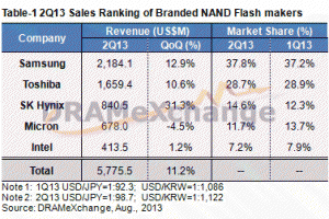
NAND prices are surging, reports TrendForce, with Q2 shipments of $5.775 billion, an 11.2% QoQ and over 30% YoY increase.
Rohm’s tiny transistor available at Mouser

Mouser Electronics has availability of what is claimed to be the smallest transistor package on the market from Rohm Semiconductor. The VML0806 case type measures just 0.8mm × 0.6mm with a height of only 0.36mm. According to Rohm, problems related to internal element miniaturisation, bonding stability, package process accuracy, and surface mount technology had limited the smallest conventional transistors to ...
Fable: The Country Which Believes In Process Technology
There was once a small country which believed in IC process technology.
Europe Off To The IC Races

It’s been an extraordinary couple of weeks for the European semiconductor industry. Three things happened:
Cavendish Kinetics MEMS Gets Actual Mbps Nearer To Theoretical Mbps
Cavendish Kinetics has an answer to the the widening gap between actual mobile data rates and theoretically achievable data rates.
Is The American Semiconductor Industry Going Home?
Is the US semiconductor industry reverting back to its early days with the East Coast becoming the new industry hub?