X-Fab has improved 25V isolation for better SPAD integration in its 180nm XH018 fab process. 4×3 SPAD arrays: Original Isomos1 and new Isomos2 (right) SPADs – single-photon avalanche diodes – are used as optical receivers in lidar, 3D imaging, depth sensing and quantum communication. The improved isolation module, called Isomos2, improves pixel density and fill factor. “In a typical 4×3 ...
Home » Tag Archives: Fabrication Semiconductors
Fabrication Semiconductors
Imec reveals CO2 assessment tool for fabs

Belgian semiconductor research lab Imec has revealed an on-line tool that quantifies the environmental impact of IC manufacturing. Called imec.netzero, it is built on an in-house virtual model of a fab and its supply chain. “The tool provides valuable insights for academics, policy makers and designers,” according to Imec, which “aims to support industry in reducing its environmental impact, beyond ...
X-Fab offers 110nm BCD-on-SoI process

Mixed-signal chip maker X-Fab Silicon Foundries is X-Fab offering a 110nm BCD-on-SoI process, claiming to be the first to do so. Called XT011, it “reflects the need for greater digital integration and processing capabilities within analogue applications”, said X-Fab, claiming: “It brings together the appealing attributes associated with both SoI and DTI [deep trench isolation], so that high-density digital logic ...
More on: Jet-powered submarine is <1mm across
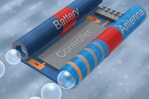
Chemnitz University of Technology has reported a steerable jet-powered micro-submarine, built using wafer processing techniques. Curious, Electronic Weekly got in touch with the team to find out more. A note on the diagram (right) – this is the best diagram of the basic structure we can get our hands on, although it is of a future concept rather than the ...
Unseasonal Rise For Semi Sales, says SIA
<p>Unusually, January semiconductor sales were up on December sales, reports the US Semiconductor Industry Association (SIA). The normal seasonal pattern is...</p>
Cardiff solar cell plant gets further $30m
Cardiff-based roll-to-roll solar cell maker G24 Innovations (G24) has raised a further $30m.
UK plastic electronics centre building finished
<p>30jul08Petec</p> <p>Building work at the Printable Electronics Technology Centre (PETEC) in Sedgefield has been completed.</p> <p>Based at NETPark, the Centre...</p>
Oxford University gets 18% more light from LCDs
The University of Oxford has developed a way to improve LCDs without complex drive techniques.
Software tunes GUI for disabled computer users
<p>Researchers at the University of Washington have developed a self-optimising graphical interface for disabled computer users.</p> <p>"Assistive technologies...</p>
PlayStation processor dominates green supercomputing
<p>Computers based on the PlayStation's Cell processor dominate the world ranking for energy efficient supercomputers, according to the just-published Green500...</p>