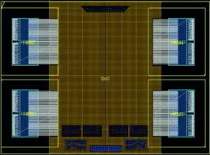
Figure 1: An SoC design with four HBMs assembled within a graphical floor planning tool
The semiconductor industry is undergoing a transformative shift towards chiplet-based architectures. This is driven by the need for higher functional density and, at the same time, a requirement for cost efficiency in ICs. One innovative approach uses hierarchical device planning and parameterised pin regions to streamline the design and manufacturing process of chiplets.
The rise of chiplet architectures
As the complexity and cost of designing monolithic ICs on advanced process nodes continue to escalate, the industry is increasingly adopting chiplet architectures. This involves disaggregating large SoCs into smaller, manageable dies or chiplets. This method not only enhances design flexibility, but also optimises power, performance and area metrics.
The traditional approach to IC design treats each device as a single flat entity. This is becoming impractical due to increasing design complexity and the need for iterative multi-physics analysis during the floorplanning stage. Hierarchical device planning breaks down the design into smaller, reusable building blocks. This allows for more efficient design iterations and easier management of complex IC packages.
One of the key innovations in hierarchical device planning is the use of parameterised pin regions. These regions define the placement and connectivity of pins in a flexible and scalable manner. By using regular expressions and design attribute tokens, designers can quickly generate and modify pin layouts, significantly reducing the time required for design updates.
These parameterised pin regions also allow for the creation of robust power distribution networks by defining and reusing power and ground pin patterns across different levels of the hierarchy. This not only simplifies the design process, but also ensures consistent power delivery across the entire IC package.
Design example
To illustrate the benefits of this approach, consider an SoC design with four HBMs (high bandwidth memories), as shown in Figure 1. In a traditional flat design methodology, any change in the power or ground pin pattern would require extensive manual updates. Using hierarchical device planning and parameterised pin regions, however, these changes can be implemented quickly and accurately. The design can be disaggregated into chiplets, each with its own hierarchical building blocks and pin regions, allowing for rapid design iterations and optimisations.
In this design, an SoC comprising four HBMs is initially assembled within a graphical floor planning tool, with several files containing fixed pin positions referenced to generate the completed design. The design is then disaggregated into chiplets, each with its own hierarchical building blocks and pin regions (Figure 2).
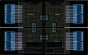
Figure 2: The original 4xHBM SoC design disaggregated into chiplets
Efficient power distribution is crucial in chiplet-based designs. Hierarchical device planning facilitates the creation of robust power distribution networks by allowing designers to define and reuse power/ground pin patterns across different levels of the hierarchy. This not only simplifies the design process, but also ensures consistent power delivery across the entire IC package.
The primary power/ground domain in a typical silicon interposer, while requiring pin counts easily exceeding 100,000 bumps, is surprisingly simple. The region will have a specific pin pattern, pad stack definition and a repeating signal assignment pattern (checkerboard or horizontal/vertical striped). A highly efficient way to represent this design structure is as a set of parameterised pin regions.
The iterative nature of IC design requires frequent updates and optimisations. Hierarchical device planning supports this by enabling quick and efficient design iterations. Tools can provide advanced graphical prototyping environments that allow designers to evaluate trade-offs and optimise designs early in the development cycle. Automation scripts further streamline the process, reducing the risk of errors and accelerating time-to-market. An example of this tool is the Innovator3D IC (i3D).
Design iteration is a major driver for the implementation of hierarchical device modelling methods. Design structures that are comprised of hierarchical building blocks can be updated quickly and fully when a change is required in one of the referenced blocks. This is also true for structures comprised of parameterised pin regions. In contrast, design updates using non-graphical IC package floorplanning flows that rely on macro-driven spreadsheets to generate bump maps can be time-consuming and error prone.
When a design is constructed using hierarchical building blocks to represent the die-to-die interfaces, along with parameterised pins to represent power distribution networks and signal patterns, the path to rearchitecting the SoC into chiplets is clear and obvious. Starting with the soft IP SoC representation, after the pins are removed, the region geometries can be quickly modified into a chiplet configuration (Figure 3).
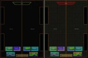
Figure 3: Silicon interposer soft IP SoC planning with parameterised pin regions: (a) prior to pin generation, (b) after VDD and VSS pins are generated
Using the same process, the pins are generated and numbered with corresponding derived signal sets. The pins in each of the four quadrants can be collectively selected and exported as a part to create a placeable building block for each chiplet. The chiplet in quadrant III, for example, can have added die-to-die interfaces for the HBM, as well as a non-proprietary representation for a high bandwidth, die-to-die building block protocol interface, such as Universal Chiplet Interconnect Express.
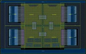
Figure 4: The top level 4xHBM_chiplet design showing the chiplet and HBM die-to-die interfaces
The completed design, after the bump pin regions have been resized and the pins regenerated, is shown in Figure 4.
The adoption of hierarchical device planning and parameterised pin regions represents a significant advancement in the design and manufacturing of chiplet-based ICs. By breaking down complex designs into manageable building blocks and leveraging flexible pin layouts, designers can achieve higher efficiency, better performance and faster time-to-market. As the semiconductor industry continues to evolve, these innovative approaches will play a crucial role in meeting the demands of next-generation ICs.
HBM explained
* High bandwidth memory can prevent bottlenecks by enabling high speed data transfer in high performance computing CPUs, GPUs and AI applications.
* It is based on a 1024-bit bus divided into channels, which are typically 8×128-bit or 16×64-bit configurations.
* To integrate HBM, complex via geometries need to be created for fanout/breakout structures for routing bits on the logic die to the HBM stack.
* Once verified, the initial channel can be used as a template that can be replicated and reused across the memory stack.