Posted on 23rd June 2025 | Modified on 26th June 2025
AI, Design, EDA and IP, Embedded Systems, News, Products, Software
All three stages of chip design will be automated and accelerated, says Moores Lab AI, which has introduced four design tools using agentic AI. Agentic AI is one of the buzzwords at this year’s DAC in San Francisco. Whereas generative AI generates content, agentic AI is an automation process. It autonomously makes and acts on decisions with little human intervention. ...
Posted on 25th February 2024 | Modified on 25th February 2024
DVCon 2024 or Design & Verification Conference & Exhibition, is the US event centred around the application of languages, tools, methodologies and standards for the design and verification of electronic systems and ICs. This highly technical conference focuses on the practical aspects of these technologies and their use in leading-edge projects. Exhibitors and presentations are designed to encourage attendees to ...
Posted on 14th February 2024 | Modified on 2nd August 2024
The Design and Verification Conference in Europe (DVCon Europe) covers the application of languages, tools and intellectual property for the design and verification of electronic systems and ICs. Chip architects, design and verification engineers, and IP integrators can explore the latest methodologies, techniques, applications and demonstrations for the practical use of EDA solutions for electronic design. The two-day event includes ...
Posted on 9th July 2018 | Modified on 25th June 2025
Test & Measurement
MediaTek has selected luton-based Anritsu’s MT8000A radio communication test station to verify MediaTek’s 5G NR mobile communication base-band chip-set. It will be used from early phase pre-silicon verification through to commercial validation of RF, protocol and function for product launch. Anritsu designed its MT8000A to work with wide-band signal processing and beam-forming, supporting sub-6GHz and millimeter-wave RF tests and as well ...
Posted on 6th July 2018 | Modified on 23rd June 2025
EDA and IP, Embedded Systems, News
Caroline Hayes finds out about the Accellera effect at DAC 2018 As well as EDA, IP and SoC companies, this year’s DAC was distinguished by the number of industry bodies that were promoting their particular brand of technology and establishing standards which the industry should follow. Accellera , the body promoting system level design, modelling and verification standards, was linked ...
Posted on 8th April 2016 | Modified on 8th April 2016
EDA and IP, News
The University of Oxford has confirmed its place as a specialist in formal verification of IC designs with the naming of Dr. Ziyad Hanna, Cadence vice president of R&D, as a visiting professor in Oxford’s Department of Computer Science for the next three years. Oxford’s Automated Verification Group has an international reputation and the appointment Dr. Hanna brings commercial experience ...
Posted on 5th April 2016 | Modified on 11th June 2019
EDA and IP, News
Cadence Design Systems has addressed verification of complex analogue IC designs with its latest Virtuoso platform. This is a recognition of the growing importance of analogue and mixed chip design for data gatheirng nodes which are part of the internet of things (IoT). The tool’s Analogue Design Environment (ADE) will be used for advanced-node designs and will be part of ...
Posted on 27th January 2016 | Modified on 16th February 2016
Automotive Electronics, EDA and IP, News
IC design house Sondrel says that automotive SoC design is now starting to focus around the 28nm process node. This is now a well-established and high yield node and so will support the automotive sector’s need for dielectric isolation (leakage current v speed trade off). This will mean that IC designers must address the design rules associated with: High Temperature ...
Posted on 11th January 2016 | Modified on 13th January 2016
EDA and IP, News
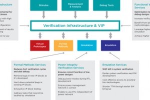
Verification technology has advanced significantly over the last few years and with today’s SoC design, verification needs to be done at all levels, from the system down to the silicon in parallel, moving up and down the levels as appropriate, writes Paul McLellan, Cadence Design Systems. The key verification technologies are formal approaches, simulation, virtual platforms, emulation and FPGA prototyping. Each technology ...
Posted on 18th December 2015 | Modified on 18th December 2015
Business
The benefits of formal verification are becoming more significant when designing modern complex ICs, says Sondrel, enabling you to verify designs earlier and more reliably, helping you achieve the desired “shift left”. The type of services that benefit from this technique include: Development of formal verification strategies,integration and optimisation of existing verification flows Provision of reusable formal verification components. Assistance ...