Home » Tag Archives: Substrate

Substrate

Substrate market to be worth $31bn by 2030

Yole-substrate-share-300x200.webp

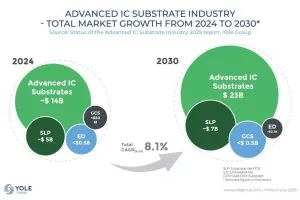
The substrate market will be worth $31 billion by 2030 driven by AI and HPC, says Yole, spanning Advanced IC Substrates (AICS), Glass Core Substrates (GCS), Substrate-like PCB (SLP), and Embedded Die (ED) technologies. The AICS market reached $14.2 billion in 2024growing 1% y-o-y; GCS is coming closer to commercialisation with strategic investments and pilot lines set up globally; SLP ...

9% CAGR 2024-29 for advanced substrate market, says Yole

The advanced IC substrate market is expected to have a CAGR 24-29 of 9% to  $25.53 billion in 2029, according to Yole Group. Competition to commercialise glass core substrates is intensifying as more players enter the field. Absolics, Intel, and Samsung are the key players, backed by a vast network of equipment, materials, and glass suppliers within their sub-supply chains. ...

Fuji joins 3d printed electronics alliance

Fuji JAMES partnership announcement

Fuji Corporation has joined 3d printed electronics association JAMES (Jetted Additively Manufactured Electronics Sources), which describes itself as establishing a collaborative community that brings together professionals and enthusiasts from various fields to drive additive manufacturing development in 3D printed electronics. The addition of Fuji “will allow both companies to work together on upcoming projects, share insights, and develop new ideas ...

ST to build SiC substrate factory in Sicily

ST 8in SiC wafer

STMicroelectronics is planning integrated silicon carbide substrate manufacturing facility on the Italian island of Sicily to support demand for SiC ICs from automotive and industrial customers. “Production is expected to start in 2023, enabling a balanced supply of SiC substrate between internal and merchant supply,” said the company, which is planning to reach 40% internal substrate sourcing by 2024. To ...

Single crystal graphene grown on sapphire

KAUST-graphene-on-sapphire3-jpg-300x200.jpg

Researchers in Saudi Arabia have grown wafer-scale single crystal graphene on insulating substrates. “If graphene can be grown on an insulating substrate with a clean interface, certain devices might function better,” said project scientist Bo Tian of KAUST – the King Abdullah University of Science and Technology. “This also opens the door to new types of graphene-based nanodevices.” The technique ...

Escatec cools high-brightness LEDs

image16-300x115-300x115.jpg

ESCATEC has a solution to the challenge of effectively cooling high brightness LEDs. Its Heat Spreader approach solders the LEDs onto a copper substrate, which is up to ten times more effective at dissipating the heat generated by the LEDs than current solutions. The CoolRunning design means that LEDs with a power density of up to 10W per mm2 could ...

Polysilicon-on-paper for printing low-cost circuits

Delft polysilicon on paper

Polysilicon can be made on paper and other low-temperature substrates by a process developer by researchers in The Netherlands and Japan. The same process has yielded CMOS transistors on a wafer. Silicon has already been used as an alternative to organic and oxide semiconductor materials in inks for printing transistors on plastic substrates using the liquid cyclopentasilane (CPS). However, getting ...

More on: Conventional components in flexible skin sensor

Last week US researchers revealed a flexible stretchable epidermal sensor made using off-the-shelf ICs, rather than custom components. In a nutshell, normal components (ground to 1mm think where needed) are mounted on an 0.3mm elastic substrate and connected together by serpentined-serpentine tracks. The substrate and circuit is capped with a flexible lid, and lubricating silicone oil injected (see image). However, ...